How to Increase the Damage Threshold of Acousto-Optic Q-Switches in High-Power Solid-State Lasers?
In high-power diode-pumped solid-state lasers (DPSS) and fiber laser systems, the intracavity acousto-optic Q-switch (AOQS) is continuously exposed to extremely high forward, reverse, and amplified stimulated emission vectors. As it acts as a variable loss element directly located within the optical cavity, it typically experiences the highest local power density in the entire system, and its state directly affects the reliability of the machine.
When the energy density of these operations exceeds the physical limit of the modulator, irreversible optical breakdown will occur. For laser developers and OEM system integrators, maximizing the laser damage threshold (LDT) of the acousto-optic switch is the most crucial factor for ensuring the long-term stability of the product and preventing on-site failures.

What Triggers Optical Damage in an Acousto-Optic Switch?
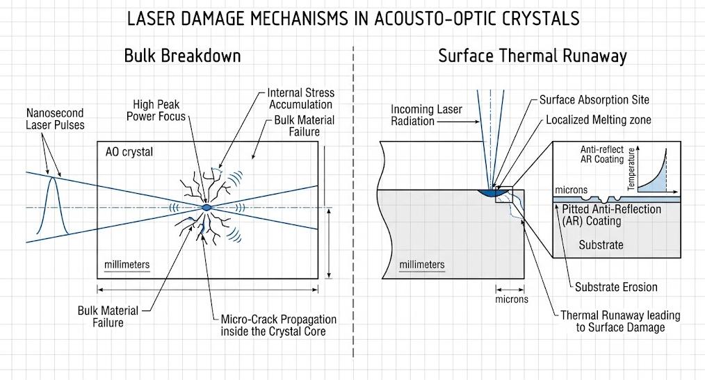
The optical performance degradation of acoustic-optic devices typically manifests in two modes: bulk dielectric breakdown and surface thermal runaway. By conducting microscopic inspections after the damage, the failure mechanism can be identified, indicating whether the problem is caused by peak power spikes or continuous average thermal loads.
Dielectric Breakdown
The damage to the body is mainly driven by the peak power density (in megawatts or gigawatts per square centimeter) during the short period of high-energy nanosecond pulses. When the local electric field of the coherent laser beam approaches the binding energy of electrons in the crystal or amorphous substrate, it triggers nonlinear absorption mechanisms, such as multiphoton ionization and avalanche ionization. This generates a high-density local plasma within the acoustic-optical interaction zone. The resulting microscopic explosion causes fractures within the crystal, leaving voids or microcracks along the propagation axis of the light beam.
Surface Thermal Runaway
Surface damage is typically a phenomenon of average power drive (measured in kilowatts per square centimeter), and structural defects at the optical interface can accelerate this process. The air-substrate interface itself is prone to being affected by environmental pollution, water absorption, and sub-surface lattice distortions left over from mechanical processing.
When the laser passes through these defect areas, there will be a slight absorption. This local heating will alter the refractive index (the thermal lensing effect) and increase the absorption coefficient of the material at that specific coordinate. This positive feedback loop – namely thermal runaway – will rapidly heat the material to its melting point or fracture point, and often leads to the peeling off of the optical coating or the formation of pits.
Key Strategies to Elevate the Laser Damage Threshold
If one wants to reduce these failure modes, precise engineering designs need to be carried out during the material procurement, optical component manufacturing, and thin film deposition stages. Among them, advanced manufacturing processes can significantly increase the laser damage threshold (LDT).
Select High-Purity Substrates
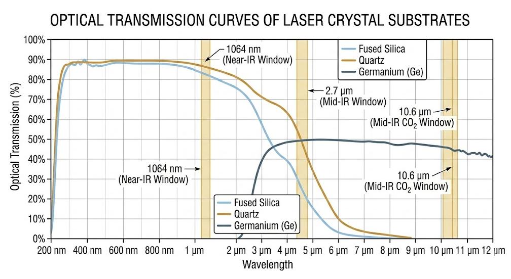
The foundation of high LDT optical devices is the raw optical medium. For lasers operating in the near-infrared spectrum (such as 1064 nm Nd:YAG or ytterbium fiber lasers), synthetic fused quartz is still the industry standard. However, standard commercial-grade synthetic fused quartz usually contains trace hydroxyl (OH⁻ ion) and metal impurities, which may introduce micro-absorption bands.
The high-power configuration requires the use of Suprasil or equivalent ultra-pure synthetic fused quartz, which are prepared by chemical vapor deposition. These materials have a uniform structure, contain almost no inclusions or bubbles, and have an extremely low absorption coefficient (less than 0.00001 cm⁻¹ at a wavelength of 1064 nm). For mid-infrared to far-infrared wavelengths, such as 2.7 micrometers Er:YAG lasers or 10.6 micrometers CO2 lasers, crystals of tellurium dioxide (TeO2) with strict crystal orientation tolerances or high-purity germanium (Ge) must be used to eliminate acoustic wave front errors, in order to avoid uneven light distribution.
Advanced Anti-reflective (AR) Coating Technology
The boundary layer between the air and the optical substrate is the lowest laser damage threshold (LDT) for all Q-switches. The traditional electron beam (E-beam) evaporation technique forms a porous coating structure with a low packing density. These micro-pores will absorb moisture and volatile organic compounds (VOC) in the atmosphere, thereby forming local high-absorption centers, which will fail under laser irradiation.
In order to operate normally in a multi-kilowatt environment, the acoustic-optical switch must adopt an ion beam sputtering (IBS) coating. IBS uses high-energy ions to deposit coating materials (such as SiO2 and HfO2) onto the substrate surface in a targeted manner. This can form a completely dense, amorphous, and completely pore-free film layer with cryptographic precision. The absorption value of the IBS coating is less than 1 to 2 ppm, which can increase the surface LDT by 3 to 5 times compared to the standard E-beam coating.
Outstanding Surface Polishing Technique
Even when using ultra-pure substrates, standard mechanical polishing still leaves a sub-surface damage (SSD) layer, including microcracks, embedded polishing abrasives, and structural stress zones. These microscopic defects enhance the electric field strength, causing the laser field intensity to be locally amplified by two or more times.
- Standard polishing (Ra greater than 0.5 nm) -> Microcracks and contaminants -> Electrostatic field amplification (damage risk)
- Super-polishing (Ra less than 0.2 nm) -> Atomic-level smooth surface -> Uniform field distribution (high laser damage threshold)
High-power components are fabricated using the ultraprecision chemical mechanical polishing (CMP) process. The ultraprecision polishing can reduce the surface roughness to Ra less than 0.2 nm. More importantly, it can systematically remove the SSD layer. This atomic-level smooth and defect-free surface treatment can prevent spatial field modulation, ensuring that the incident laser energy is uniformly distributed over the optical aperture without encountering local hotspots.
Optimizing Laser Parameters and Cooling for Longevity
Manufacturing control determines the theoretical breakdown limit of the device, while the actual service life depends on the active heat dissipation and geometric management during the system integration process.
Active Cooling Design
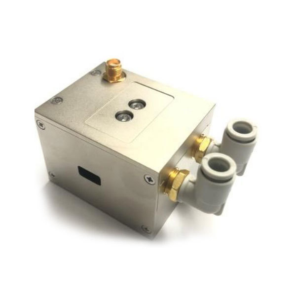
The optical and acoustic Q-switch will convert most of the input RF energy into internal waste heat. For lasers with an average power exceeding 20W, passive conduction cooling is insufficient to meet the requirements. The system design must adopt active water cooling, using an oxygen-free high thermal conductivity (OFHC) copper block directly integrated into the housing. Maintaining a stable layer flow can stabilize the overall temperature of the crystal, minimize the thermal lens effect, and prevent mechanical stress fractures at the transducer interface.
Beam Expanding and Spot Size Optimization
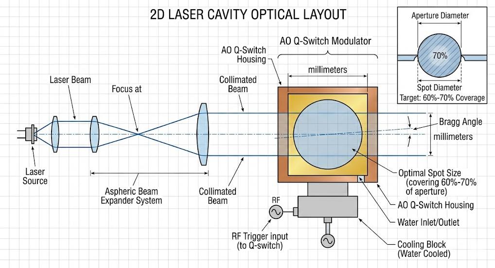
Focusing the laser beam too tightly inside the Q-switch can cause the local power density to rise rapidly, accelerating surface and overall breakdown. On the contrary, an overly large beam may result in the cutting off of peripheral light spots and diffraction scattering onto the transducer housing. Integrators should use an intracavity beam expander to adjust the beam diameter, making it occupy 60% to 70% of the designated light aperture of the device. This configuration can maintain the fast acoustic rise time required for an efficient Q-switch while ensuring that the energy density is below the catastrophic threshold.
High-Power Acousto-Optic Q-Switch Selection Matrix
In designing or acquiring parts for incorporation in laser systems that are either industrial or scientific in nature, use the following engineering parameters to match the system’s power requirements:
| Mitigation Factor | Standard Specification | High-Power Optimized Spec | Key LDT Benefit |
| Substrate Grade | Commercial Optical Fused Silica | Synthetic Fused Silica (Suprasil) | Eliminates internal inclusions and minimizes bulk absorption. |
| Surface Finish | Ra less than 0.5 nm | Super-Polished (Ra less than 0.2 nm) | Removes sub-surface damage to prevent electric field hotspots. |
| Coating Type | E-Beam Evaporation (Porous) | Ion Beam Sputtering (IBS) | Lowers surface absorption below 2 ppm, stopping thermal runaway. |
| Cooling Method | Conduction / Air Cooled | Active Water-Cooled (OFHC Copper) | Dissipates RF and optical waste heat to eliminate stress fractures. |
| Aperture Design | Unoptimized Spot Size | Controlled Spot (60% to 70% of Aperture) | Reduces peak power density while protecting transducer margins. |
The requirement of high diffraction efficiency together with good metrics in terms of laser damage threshold necessitates stringent control in vertical integration of crystal alignment, surface polishing, and thin-film coating. In case of any queries related to engineering consults for apertures, wavelength (2.7-10.6 microns) specification, or high RF driver power, please contact SMART SCI&TECH.